
Test the Quality of PCB Design Assembly
The quality of PCB design assembly is essential for ensuring that the finished product functions properly. PCBs are subjected to intense physical and environmental stresses during manufacturing, testing and use, so it is vital that they meet strict quality control standards throughout each stage of the process. This ensures that the end-product is free from external faults and defects.
The most common way to test a pcb design assembly is through manual visual inspection. This involves examining the board with the naked eye or through magnification and comparing it to the original design files to ensure that all specifications are met. This method can catch a wide range of surface errors, including footprint pad-component misalignment, tombstoning, and more.
In-circuit test (ICT) is another popular form of testing, which uses fixed probes arranged in a pattern matching the PCB’s layout to examine solder connections. This type of testing can detect a range of problems, such as shorts between pins and islands, open copper traces, and solder bridges.
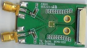
How Do You Test the Quality of PCB Design Assembly?
X-ray inspection is another form of testing that allows manufacturers to examine internal components and connections on a printed circuit board. This method can also identify solder bridges, open copper traces, and cold solder. It is often used in combination with other inspection methods, such as flying probe or ICT, to ensure that all parts are correctly positioned and secured to the PCB.
Functional testing aims to simulate a product’s operation and performance, so it can discover any problems before they become major issues. This type of test can include testing for EMI and temperature cycling, as well as tests that analyze how well a PCB performs in an extreme environment, such as high humidity.
The PCB design process starts with conceptualizing the board layout. Engineers and designers use Computer-Aided Design (CAD) software to create a blueprint that defines the electrical paths, placement of components, and the overall structure of the PCB. This initial design phase involves several stages.
A key component of PCB manufacturing is the Gerber file, which provides detailed information about the layers of a circuit board’s design. It also contains instructions about how to assemble each part on the board. This is important because a faulty file can cause a variety of problems during the manufacturing process, such as incorrect routing and soldering. This can lead to costly repairs and a shortened life for the end-product. To avoid this, a manufacturer should review and verify all files prior to the beginning of production. Moreover, the manufacturer should provide thorough documentation of each step of the manufacturing process to ensure quality.

